iPad ProのA9XにはセミカスタムモデルのPowerVR Series7XT 12Coreモデルが採用されているようです。詳細は以下から。
![]()
投資情報を専門に扱うThe Motley FoolのAshraf EassaさんがChipworksから得た情報によると、AppleがiPad Proに採用したApple A9XプロセッサにはiPhone 6sシリーズの倍の12-Core GPUが搭載され、L3キャッシュが無くなっているとのことです。
After contacting the folks at Chipworks, I was able to get some interesting information about the A9X chip that powers the recently launched iPad Pro as well as a die shot of the chip that I am allowed to publish for your viewing pleasure.
Inside the Apple Inc. A9X Chip – The Motley Fool
A8~A9の比較
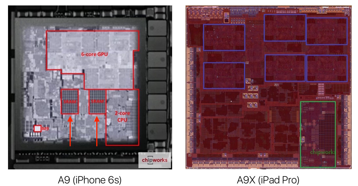
The Motley FoolがICチップの特許支援や特許侵害を調査を行っているChipworksのDick Jamesさんから得た情報によると、iPad Proに搭載されているApple A9XはiPhone 6sシリーズのApple A9と同様に14/16nmプロセスが採用されており、コア数もA9と同じ2-Coreなものの(下記画像は1ブロックが2-CoreでA9XのCPUは緑、GPUは青のブロック)
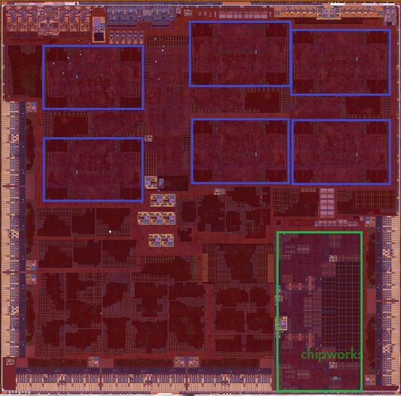
Chipworks’ Dick James tells me that he sees a 12-cluster GPU, two CPU cores, and an absence of the level-three cache memory found inside the A9 chip (I’ll explain why I think Apple didn’t include it later in this article). I agree with his assessment. The two CPU cores can be seen in the green box, and I believe that inside of each blue box are two GPU clusters, for a total of 12 clusters.
Inside the Apple Inc. A9X Chip – The Motley Fool
GPU数はA9の倍の12-Core(クラスター) GPUが採用されているそうで、このGPUがMacBook Pro (Retina, 15-inch, Late 2013)と同程度のエンコードパフォーマンスを提供しているようです。
| iPhone 6 | iPad Air 2 | iPhone 6s | iPad Pro | |
|---|---|---|---|---|
| GPU | PowerVR GX6450 | PowerVR GXA6850 | PowerVR GT7600 | PowerVR 7XT Custom |
| Core数 | 4 | 8 | 6 | 12 |
| ALU | 128 (FP32) | 256 (FP32) | 192 (FP32) | ??? |
| プロセスルール | 20 nm | 20 nm | 14/16 nm | 14/16 nm |
| API Support | OpenGL® ES 1.x/2.0/3.x* OpenGL 4.x* DirectX10_0 OpenCL™ 1.2 EP* Renderscript |
OpenGL® ES 1.x/2.0/3.x* AEP OpenGL 3.3* DirectX 10_0 OpenCL™ 1.2 EP* (DirectX 11_2,OpenGL 4.3*,OpenCL 1.2 FP*) |
||
| リンク | Imagination NotebookCheck |
Imagination NotebookCheck |
Imagination NotebookCheck |
Imagination |
また、JamesさんはImagination Technologies社のPowerVR Series 7XTシリーズのラインナップに注目しており、それによるImagination Technologies社が公開しているPowerVR Series 7XT GPU Familyの情報にはGPU Core数(shading clusters)が2, 4, 6, 8, 16の情報が記載されているものの、
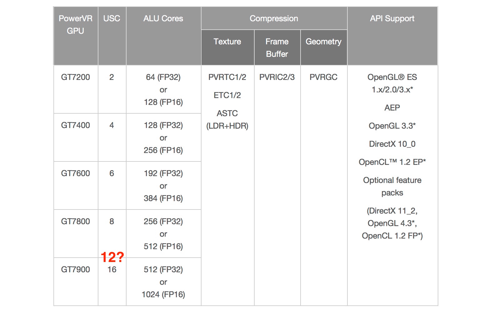
One thing worth noting is that Imagination Technologies — Apple’s GPU IP supplier — only lists variants of its Series 7XT graphics IP with 2, 4, 6, 8, and 16 “shading clusters.” The 12-cluster design points to a semi-custom implementation by Apple of the Series 7XT, similar to what Apple did with the Series 6XT-based graphics IP in last year’s A8X chip.
12-Coreの情報はどこにもないため、A9Xに採用されているPowerVR Series7XT GPUはAppleがImagination Technologiesに発注したセミカスタムモデルではないかと予想しており、これらを搭載するためA9XのダイサイズはA9より約40%程大きい147平方mm程度になっているそうです。
According to Chipworks, the chip measures in at approximately 147 square millimeters, a whopping 40% larger than the size of the TSMC-built variant of the A9 chip inside of the iPhone 6s/6s Plus. This is an absolutely huge increase in area (and by extension transistor count) from the A9, which no doubt means that this monster of a chip is far more difficult to manufacture, especially on a relatively new manufacturing technology.
Inside the Apple Inc. A9X Chip – The Motley Fool
L3キャッシュ
A9XではさらにA9に存在した8MBのオンボードL3キャッシュが無くなっており(左図の中央)、これについてはA9XがA8Xの2倍のメモリ幅(128-bit, 51.2GB/sec)を持ったLPDDR4を採用したことにより不要になったのではないかとEassaさんは予想しており、
Connecting the lack of cache with die size
Remember how I said that it doesn’t look like the A9X features the 8 megabytes of on-die cache memory that the A9 does? Well, I think I have an explanation for that.
The A9X features a memory interface that’s twice as wide as the one on the A9, allowing the chip to pass data to and from memory at twice the rate that the A9 can.Inside the Apple Inc. A9X Chip – The Motley Fool
これはiPad Proが広大な排熱空間と設置空間を確保できたため、ダイとメモリをボード上で分けることに成功したのではないかと推測しています。
I believe that this is enabled by the fact that a chip like the A9X, which powers a relatively large device such as the iPad Pro, has both more thermal headroom than the A9 (since the iPad Pro is a larger device that can handle a more power hungry chip) and can take up a larger area footprint than a phone chip (the memory inside of the iPhone 6s/6s is stacked on-top of the A9 package; the memory in the iPad Pro sits on the logic board).
Inside the Apple Inc. A9X Chip – The Motley Fool
ChipworksではまだA9Xの調査レポートが公開されていませんが、The Motley FoolはA9Xの様な複雑なチップは製造が難しく、現在の最高クラスのCPUだろうとレポートしているので興味がある方は関連リンクからThe Motley Foolの記事へどうぞ。
関連リンク

コメント
L3がL2に吸収されたか…
まあ、これはiPadシリーズだからできることで、スモールファクタのiPhoneにはしばらく無理だろうけど何か感無量だな。
>>1
PowerPC 970もL3なかったよね〜
あの時はベンチマークスコアの結果が振るわなくてもめた記憶があるけど、IPad Proはそんなことないのかな?
Tegra X1に相当?
あれはデスクトップ用だけどね。
GFX Benchの1080p Manhattan offscreenで比較すると
iPad Proが80FPS
X1チップが64FPS
iPad Air2が43FPS
かなりiPad Proって凄いんだな。
LPDDR4のRAMを搭載してるiPhone6sには何でL3キャッシュがあるの?
>>5
実際のところはわからないけど、要素の開発と全体の開発は必ずしも同期しない
DDR4を採用しない可能性があったか、CPUの大規模設計変更が間に合わない予測があったか、L3廃止の影響評価が間に合わない可能性があったか
全部に新機軸を盛り込むとガタガタになりやすいから少しずつ変えるやり方の方が製造系では好まれる
>>5,6
品質評価のあるだろうけど、iPad Proの場合は単にパッケージサイズの問題じゃないかな?
iPad Proは広大なフリースペースがあるわけだし、自由にメモリやA9Xの大きさを設定できるてのが大きいと思う。
オンボードじゃなくてオンダイでは?
>>5だけど、iPad Proだから出来る事なんだね
L3キャッシュってあった方がいいの?それとも無い方がいいの?
L3キャッシュは8MBじゃなく4MBだそうです
L3は8MBじゃなく4MBが正しそうです
プロセッサの速度に対してメインメモリが十分に高速ならキャッシュは不要だし無いほうが自然。メモリのコヒーレンシを維持するコストもタダじゃないしね。